- 您现在的位置:买卖IC网 > Sheet目录3887 > PIC16F1825-E/ML (Microchip Technology)MCU PIC 14K FLASH 1K RAM 16QFN
137
ATmega8515(L)
2512K–AVR–01/10
AVR USART vs. AVR UART –
Compatibility
The USART is fully compatible with the AVR UART regarding:
Bit locations inside all USART Registers
Baud Rate Generation
Transmitter Operation
Transmit Buffer Functionality
Receiver Operation
However, the receive buffering has two improvements that will affect the compatibility in
some special cases:
A second Buffer Register has been added. The two Buffer Registers operate as a
circular FIFO buffer. Therefore the UDR must only be read once for each incoming
data. More important is the fact that the Error Flags (FE and DOR) and the ninth
data bit (RXB8) are buffered with the data in the receive buffer. Therefore the status
bits must always be read before the UDR Register is read. Otherwise the error
status will be lost since the buffer state is lost.
The Receiver Shift Register can now act as a third buffer level. This is done by
allowing the received data to remain in the serial Shift Register (see Figure 64) if the
Buffer Registers are full, until a new start bit is detected. The USART is therefore
more resistant to Data OverRun (DOR) error conditions.
The following control bits have changed name, but have same functionality and register
location:
CHR9 is changed to UCSZ2
OR is changed to DOR
Clock Generation
The clock generation logic generates the base clock for the Transmitter and Receiver.
The USART supports four modes of clock operation: Normal asynchronous, Double
Speed asynchronous, Master synchronous and Slave synchronous mode. The UMSEL
bit in USART Control and Status Register C (UCSRC) selects between asynchronous
and synchronous operation. Double Speed (asynchronous mode only) is controlled by
the U2X found in the UCSRA Register. When using Synchronous mode (UMSEL = 1),
the Data Direction Register for the XCK pin (DDR_XCK) controls whether the clock
source is internal (Master mode) or external (Slave mode). The XCK pin is only active
when using Synchronous mode.
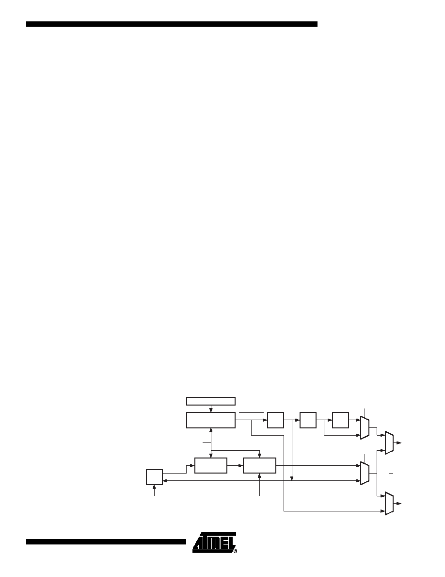
Figure 65 shows a block diagram of the clock generation logic.
Figure 65. Clock Generation Logic, Block Diagram
Prescaling
Down-counter
/2
UBRR
/4
/2
fosc
UBRR+1
Sync
Register
OSC
XCK
Pin
txclk
U2X
UMSEL
DDR_XCK
0
1
0
1
xcki
xcko
DDR_XCK
rxclk
0
1
0
Edge
Detector
UCPOL
发布紧急采购,3分钟左右您将得到回复。
相关PDF资料
PIC16F1828-I/SO
IC PIC MCU 8BIT 14KB FLSH 20SOIC
PIC16F688-I/SL
IC PIC MCU FLASH 4KX14 14SOIC
22-02-3213
CONN FFC/FPC VERTICAL 21POS .100
22-15-3193
CONN FFC/FPC 19POS .100 RT ANG
PIC16C433T-E/SO
IC MCU CMOS 8BIT 10MHZ 2K 18SOIC
22-02-3103
CONN FFC/FPC VERTICAL 10POS .100
PIC16C432T-E/SS
IC MCU CMOS 8BIT 20MHZ 2K 20SSOP
PIC16C432-I/P
IC MCU CMOS 8-BIT 20MHZ 2K 20DIP
相关代理商/技术参数
PIC16F1825-E/ML
制造商:Microchip Technology Inc 功能描述:; Controller Family/Series:PIC16F; Core
PIC16F1825-E/P
功能描述:8位微控制器 -MCU 14KB FL 1KBRAM 32MHz 12I/0 Enhanced Mid RoHS:否 制造商:Silicon Labs 核心:8051 处理器系列:C8051F39x 数据总线宽度:8 bit 最大时钟频率:50 MHz 程序存储器大小:16 KB 数据 RAM 大小:1 KB 片上 ADC:Yes 工作电源电压:1.8 V to 3.6 V 工作温度范围:- 40 C to + 105 C 封装 / 箱体:QFN-20 安装风格:SMD/SMT
PIC16F1825-E/P
制造商:Microchip Technology Inc 功能描述:; Controller Family/Series:PIC16F; Core
PIC16F1825-E/SL
功能描述:8位微控制器 -MCU 14KB FL 1KBRAM 32MHz 12I/0 Enhanced Mid RoHS:否 制造商:Silicon Labs 核心:8051 处理器系列:C8051F39x 数据总线宽度:8 bit 最大时钟频率:50 MHz 程序存储器大小:16 KB 数据 RAM 大小:1 KB 片上 ADC:Yes 工作电源电压:1.8 V to 3.6 V 工作温度范围:- 40 C to + 105 C 封装 / 箱体:QFN-20 安装风格:SMD/SMT
PIC16F1825-E/SL
制造商:Microchip Technology Inc 功能描述:; Controller Family/Series:PIC16F; Core 制造商:Microchip Technology Inc 功能描述:IC, 8BIT MCU, PIC16F, 32MHz, SOIC-14
PIC16F1825-E/ST
功能描述:8位微控制器 -MCU 14KB FL 1KBRAM 32MHz 12I/0 Enhanced Mid RoHS:否 制造商:Silicon Labs 核心:8051 处理器系列:C8051F39x 数据总线宽度:8 bit 最大时钟频率:50 MHz 程序存储器大小:16 KB 数据 RAM 大小:1 KB 片上 ADC:Yes 工作电源电压:1.8 V to 3.6 V 工作温度范围:- 40 C to + 105 C 封装 / 箱体:QFN-20 安装风格:SMD/SMT
PIC16F1825-E/ST
制造商:Microchip Technology Inc 功能描述:; Controller Family/Series:PIC16F; Core 制造商:Microchip Technology Inc 功能描述:IC, 8BIT MCU, PIC16F, 32MHz, TSSOP-14
PIC16F1825-I/ML
功能描述:8位微控制器 -MCU 14KB FL 1KBRAM 32MHz 12I/0 Enhanced Mid RoHS:否 制造商:Silicon Labs 核心:8051 处理器系列:C8051F39x 数据总线宽度:8 bit 最大时钟频率:50 MHz 程序存储器大小:16 KB 数据 RAM 大小:1 KB 片上 ADC:Yes 工作电源电压:1.8 V to 3.6 V 工作温度范围:- 40 C to + 105 C 封装 / 箱体:QFN-20 安装风格:SMD/SMT